
KiCad is an electronic design automation (EDA) application that helps users create electronic schematics and printed circuit board (PCB) layouts. Designed for engineers, electronics enthusiasts, and hardware developers, it provides tools for designing circuits, creating PCB layouts, analyzing board files, and viewing designs in 3D. The software combines schematic editing, PCB design, component libraries, measurement tools, and manufacturing-related utilities into a single platform. Despite offering many advanced features, KiCad maintains a clean interface that makes the workflow accessible for users working on electronic projects.
Features of KiCad
Schematic Design Tools
- Create and edit electronic schematic diagrams
- Configure page settings
- Perform standard editing operations including cut, copy, paste, and delete
- Undo and redo design changes
- Zoom and navigate schematic layouts
- Draw wires and buses in any direction
- Add local and global labels
- Insert circuit junctions
- Select components from built-in libraries
- Check circuit validity with error and warning reports
- Choose measurement units
- Print circuit designs
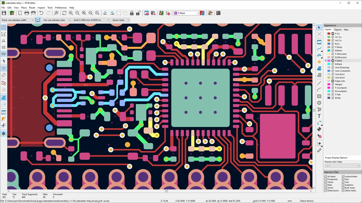
PCB Layout Design
- Create printed circuit board layouts
- Configure PCB design rules
- Work with multiple PCB layers
- Add tracks, zones, arcs, circles, and polygons
- Manage PCB footprints
- Upload NET files
- View selected footprints
- Switch between PCB editing and 3D visualization
- Print PCB designs
- Export boards to DSN, CAD, and WRL formats
3D Visualization and Analysis
- View PCB designs in 3D mode
- Inspect board structures visually
- Analyze PCB appearance before production
Additional Tools
- Access and analyze Gerber files
- Review copper layers, solder masks, legends, and drill holes
- Create logos from BMP images
- Record macros
- Assign custom hotkeys
- Save projects as ZIP files
- Use an external text editor
- Access PCB calculator tools
User Experience
KiCad provides a complete workflow for electronic design, starting from schematic creation and continuing through PCB layout and board analysis. The software interface is organized around dedicated design tools, allowing users to move between circuit diagrams, PCB layouts, and 3D visualization.
The schematic editor is straightforward to use for creating and modifying circuits. Basic editing functions are easy to access, while more advanced options such as labels, junctions, component libraries, and circuit validation tools provide the flexibility needed for detailed projects. The PCB editor is where KiCad becomes especially valuable for hardware designers. Users can work with multiple layers, define design rules, place tracks and zones, and inspect layouts before manufacturing. The 3D viewer adds another level of convenience by allowing users to visualize the finished board design.
The availability of Gerber file analysis tools is also useful for reviewing manufacturing outputs. Being able to inspect copper layers, solder masks, legends, and drill information within the same application helps streamline the design process. Although KiCad includes many professional features, beginners may need time to understand the workflow and terminology associated with PCB design. However, users willing to learn will find a capable platform for creating complex electronic designs.
Who Should Use KiCad?
- Electronics engineers
- PCB designers
- Hardware developers
- Electrical engineering students
- Makers and electronics hobbyists
- Professionals creating custom circuit boards
- Users looking for a complete electronic design workflow
Conclusion
KiCad offers a comprehensive environment for designing electronic circuits and printed circuit boards. With schematic editing, PCB layout, 3D visualization, Gerber analysis, and customization features, it provides the tools needed for the complete hardware development process.